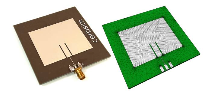
Convert Gerber files to a simulation-ready STEP file with full copper geometry (defeatured) — free tool for EM simulation.
blog.hirnschall.net


When trying to build a truly silent home server, choosing a backplane is hard. They are typically either built into a case which does not isolate vibrations and sound the way they should or they are way too expensive and hard to find.
So, let's design our own, custom 4x SATA backplane. The difficult part is designing the PCB itself. Once this is done it will be extremely cheap and also not hard to solder.
As the design is already done, you can download the gerber files (fabrication data) for the backplane on GitHub and order it on JLCPCB. The exact order details can be found on github as well.
In this post we will go over each design decision, signal integrity, electromagnetic interference, and manufacturing considerations.
Fig. 1 shows the assembled backplane. Note that the red wires in the back are a prototype issue which is fixed in the current, released version.

Before we get to the actual PCB design, let's write down a list with features we want. As the project is quite simple, we will provide the list without too much discussion.
The most important requirement, however, is that the backplane does not increase error rates.
Now that we have a list of requirements, we can start talking about design considerations. As SATA is "high speed", we have to keep an eye on signal integrity and electromagnetic interference.
SATA III operates at a data rate of 6 Gbps, which corresponds to a frequency of 3 GHz. However, the frequency we need to design for is not 3 GHz! The actual frequency lies in the rise and fall times of the signals. We see this when using fourier analysis for the rectangular waveform. A fast rise and fall time results in higher frequency components, which can lead to electromagnetic interference and signal integrity issues.
The highest frequency component of the signal we will consider is called the knee frequency and given by $$\begin{align} f_{knee} := \frac{0.35}{t_r} \end{align}$$ where \(t_r\) is the rise time of the signal (\(20\%\text{ to }80\%\)). For SATA III, the rise time is typically around 50 ps, which gives us a knee frequency of around 7 GHz [2]. This means that we need to design our backplane to handle frequencies up to 7 GHz to ensure signal integrity and minimize electromagnetic interference. For fr4 with \(\varepsilon_r = 4.4\), this leads to a wavelength $$\begin{align} \lambda = \frac{c}{f_{knee} \sqrt{\varepsilon_r}} \approx 0.02 m \end{align}$$ where \(c\) is the speed of light.
As a rule of thumb, the trace will start to behave like a transmission line when its length exceeds \(\lambda/10=0.002 m\), which it clearly will.
SATA uses differential signaling to improve signal integrity and reduce electromagnetic interference. Here two wires carry the signal with opposite polarity (simplified: one wire carries the signal, the other carries the inverted signal).
This works in the following way: The receiver looks at the difference between the two signals, which will cancel out any noise that is common to both signals. So, if a electromagnetic wave induces a voltage on both traces (which it should as we route them next to each other), the receiver will compute the difference between the two signals, which will cancel out the common mode noise and allow the receiver to correctly interpret the original signal.
For this to work, we will route the traces as differential pairs. The ECAD software typically has a tool to do exactly this.
Note: There are several discussions about the necessity to actually route the differential pair next to each other. We will not add to this here and go with the standard approach of routing them next to each other.
In this design: Primary concern.
As discussed above, the idea is to cancel out interference by computing the difference between the two signals. However, if the signals have a different propagation delay, this can lead to timing issues and reduced signal integrity.
Consider the following example: We emit a signal on both traces. Then the pair has a corner. Obviously, the signal will take longer to propagate on the outer (longer) trace than the inner one. We now have a timing mismatch. The two signals do not arrive at the same time.
If the receiver now computes the difference between the two signals, they do not align properly, causing issues with signal integrity.
To mitigate this issue we have to make sure the signal takes the same amount of time to propagate on both traces. This is often called length matching, as the two traces are made to have the same physical length. Length is often used as a practical proxy for propagation delay. Strictly speaking, however, we must match the actual propagation delay, not just the physical length.
Continuing with the example shows exactly where delay matching must be applied and what goes wrong if we apply it at the wrong spot. If a voltage is induced on both traces after the first corner, the receiver will still cancel out the common mode noise. However, if we now match the delay before the receiver to realign the signals, we also realign the noise (together with the signal) such that it no longer arrives at the receiver at the same time on both traces. The noise is thus now no longer common mode and it is therefore not canceled out by the difference computation.
To avoid this issue, we must match length/delay close to the point where the mismatch occurs.
The sata standard specifies this intra-pair skew to be \(\leq 10 ps\) [3].
In this design: Primary concern.
Another thing to mention is the propagation delay, which is the time it takes for a signal to travel along a trace.
The reason why length matching is technically not correct is that the signals may travel at different speeds through the two traces. The easiest way for this to happen is if we were to route one trace on an internal and one on an external layer (which we are obviously not doing). However, this is not the only reason the signal might travel at different speeds.
Consider the way a PCB is actually built. We have copper layers and inbetween glass fiber prepreg layers. The prepreg is a composite made from woven glass fibers and resin. Depending on if the trace is above glass fiber or above resin will affect the propagation speed.
The weave is typically oriented in \(0^\circ\) and \(90^\circ\). So, if we route our pair horizontally, One trace could be above a fiber strand and the other above resin. To combat this issue, we may align the layout to \(45^\circ\) and route the traces at \(\pm 45^\circ\). This way the differential pair is on average equally above both materials.
Another possibility is to rotate the whole PCB in CAD by around \(10^\circ\).
We have mentioned this for completeness sake but we will not consider this in this specific PCB design for SATA.
In this design: Not critical.
Crosstalk is the unwanted coupling of signals between adjacent traces. If we route two traces (not differential pair) next to each other, the signal in one can couple into the other, causing ovious issues.
The best way to avoid this issue is to maintain adequate spacing between traces. More is better but we will go with the rule of thumb:
In general, we will avoid routing traces in parallel over a large distance as it will increase the amount of crosstalk. If we have to cross other signal traces we should do so at right angles.
We take a more critical look at trace spacing and its effect on crosstalk in section 5 below where we simulate the finished PCB and a spacing example using FEM.
In this design: Primary concern.
In a transmission line, return currents flow through the ground plane to complete the circuit. The current will take the path of least impedance. For fast digital signals, due to capacitance effects, the return current will flow directly under the signal trace. It will not necessarily take the shortest path through the ground plane.
This is something we have to keep in mind when routing. We do not want to split the reference plane (ground directly under the signal trace) and thus interfere with the return current paths.
Again, consider the following example: We route a trace on the internal layer below the signal trace. As we have created a discontinuity in the reference plane, the return current has to take a detour around the slit. It will travel along the slit back and forth, creating in essence a slit antenna.
If the length of the slit approaches \(\lambda/4\), it will start to act as an antenna and radiate energy. Even if we do not match \(\lambda/4\), we have still increased the loop area which is proportional to the radiation efficiency.
In this design: Primary concern.
As we are dealing with a transmission line, we need to ensure that the impedance of the trace matches the impedance of the source and load. This helps to minimize reflections and maximize power transfer.
For SATA the differential impedance is specified as 100 ohms [3].
As we want to order from JLCPCB we will use a 4-layer board even though we only need two layers. The reason is that a two layer board is constructed differently from a multi layer board.
A typical pcb is \(1.6 mm\) thick. Thus on a two layer board the top and bottom layers will be \(1.6 mm\) apart. For multi layer boards however, a thick core is used then copper layers are separated by a thin dielectric (prepreg) layer. For the stackup we will use (JLC04161H-7628) the top layer is only \(0.2104 mm\) apart from the In1 layer. This allows us to use much thinner traces to achieve the desired impedance (think about capacitance as a function of area and distance).
We start by choosing an acceptable trace spacing. Then we can use the JLC impedance calculator to compute differential pair spacing/width to achieve the desired \(100 \Omega\). For our stackup:
In this design: Primary concern.
Now that we have computed the required trace dimensions, we have to ensure that the impedance remains constant throughout the transmission line. One possible issue are corners or vias that can cause impedance variations.
Let's start with corners. The problem here is that the cross-section of the trace changes at the corner, which can lead to impedance variations. For the speeds we are concerned about this effect is probably negligible. However, a \(45^\circ\) is better than a \(90^\circ\) corner and an arc (fillet) is better than a \(45^\circ\) corner. We will go with the arc.
Vias also cause an impedance mismatch. For this project we do not need to use vias in data lines so this is not an issue we have to consider.
Connectors and other passive components can also cause impedance mismatches. So can the pads they are attached to. We will keep pads and footprints as small as possible.
In this design: Not critical.
As mentioned above, the return current flows in the reference plane below the signal trace. If we were to use vias in our signal traces, the signal would change its reference plane. We therefore need to place ground vias next to the signal wire to allow the return current to change planes as the signal does.
Thus, we will always use vias in pairs. If we use a via, we will place a ground via next to it.
In this design: Avoided by layout.
Stubs are short sections of trace that branch off from the main transmission line. They cause unwanted reflections and if they are longer than \(\lambda/20\) to \(\lambda/40\) (again, rule of thumb) signal integrity issues. We will avoid stubs in our design and, if we have to use them, keep them as short as possible.
A non obvious cause of stubs are vias when routing on internal planes. If we were to go from one internal layer to another, the via would still go from the top of the pcb to the bottom. It would not be connected to the top and buttom layer but it would create a stub. Depending on the frequency/wavelength we are working with and the length of the stub this could be an issue.
If we determine that via stubs are an issue, we can opt for back drilling. The manufacturer would then drill away the unwanted part of the via, removing the stub.
Again, we will route on the top and bottom layers and there is no reason to use vias in this design. But it is something to keep in mind when working with high-frequency signals.
In this design: Avoided by layout.
Via fencing is a technique used to reduce electromagnetic interference by placing a row of ground vias around the signal traces. This creates a sort of "fence" that helps to contain the electromagnetic fields and reduce crosstalk between adjacent traces.
We will not use via fencing in this design. We want the differntial traces to couple to the reference plane and to each other, nothing else.
Placing ground vias around the signal traces can surely help, however, if they are too close to the signal traces, they can cause unwanted coupling, they could cause standing waves etc. We would have to carefully consider the placement and spacing of these vias.
For this design, I will therefore avoid using via fencing and go with adequate spacing instead.
Another technique to consider is PCB edge via stitching. Here ground vias are placed around the PCB edge, connecting the top to the bottom plane and creating sort of a fence. The reasoning is the following: If we use vias on signal traces, they will radiate perpendicularl to the via itself, causing a wave to travel longitudinally in the dielectric with the planes above and below as a waveguide. The wave will then exit through the edges of the PCB. If we place vias there, the wave cannot exit. We could also get the edge plated by the manufacturer.
Again, an interesting approach but in my opinion not necessary for this design. We do not use vias on the signal traces and thus we do not need to contain waves emitted by them.
In this design: Not critical.
Many RF designs remove the solder mask from the signal traces as it is not invisible to high frequency signals. It will affect the impedance and increase dielectric losses. Controlling solder mask thickness is also not easy during manufacturing.
However, to avoid corrosion we would probably have to go with ENIG (Electroless Nickel Immersion Gold). Furthermore, removing the solder mask from a PCB that goes inside a PC is not a good idea as it increases the risk of shorting traces. Lastly, the solder mask will not be an issue at the frequency range we are in.
Thus, we will keep the solder mask on the PCB.
In this design: Not critical.
There are a few sata specific considerations for our design.
Pin 11 of the SATA power connector is used for staggered spin-up and the drive activity indicator LED. If pin 11 is pulled low, staggered spin up is disabled.To support staggered spin-up, we will connect pin 11 to the 5V rail through a pull-up resistor (R1). This allows the drive to spin up when the sata controller tells it to, allowing for staggered spin-up of multiple drives. We do this similarly to [3, 4]
Fig. 2 shows the schematic for this connection. 1_ACT is the connection to pin 11 of disk 1.

SATA uses AC coupling capacitors (typically \(100 nF\)) to isolate the DC component of the signal while allowing the AC component to pass through. This way each side can set its own DC bias. In our design we will not add any additional capacitors as they are already present on the host side.
SATA supports hot plugging, which is primarily enabled by the staggered pin lengths of the standard power connector, ensuring that ground and pre-charge pins make contact before the main power and signal pins. Since this backplane uses standard SATA power connectors, it inherits this sequencing behavior. In typical desktop systems, power supplies are designed to directly handle drive insertion and the associated inrush currents, so this design behaves electrically similar to a passive Molex-to-SATA adapter. However, as discussed on GitHub and Section 6.14.3 of the SATA specification [3], fully compliant hot-plug implementations may include additional measures such as controlled inrush current and signaling considerations. These are not implemented here, meaning that while hot plugging works in practice, this design does not provide the robustness of enterprise-grade backplanes.
Now that we have gone over the design considerations, we can start designing the PCB. We will use KiCad for this project. The design files are available on GitHub.

Figure 3 shows the routing for the schematic shown in fig. 2. We use planes for power distribution, whick traces and multiple vias. Furthermore, we make sure to offset the activity LED from the hard drive so that it is actually visible.

Figure 4 is more interesting. We apply everything discussed in section 3. The signal traces are routed as differential pairs, the corners have fillets, delay matching is done close to the corners, and the two differential pairs have ample spacing between them. We have a solid ground plane on In1 directly under the signal traces. The top layer has no co-planar plane, just the differential pairs. Furthermore, no vias in the signal traces were required.
To be more exact, the spacing between the differential pairs is around \(3.1mm\) which is roughly \(15w\). The intra-pair skew is kept to \(0.001mm\) and the two differential pairs have a length mismatch (inter-pair skew) of around \(6mm\) between them. This inter-pair skew is not critical and not specified in the SATA specification.
Before we finish with the mechanical design for this project, I'd like to simulate the PCB itself and also how spacing affects cross-talk. To do so, we can use 3D FEM to compute the impedances and analyze the resulting S parameters.
First, we will convert the fabrication output (gerber files) from KiCad to a simulation ready 3D model using the free Gerber-to-STEP converter. We will then solve Maxwell's equations for the 3D model using FEM (full wave field solver) with PEC (perfect electrical conductor) boundary conditions for the copper layers and PML (Perfectly Matched Layer) to avoid reflections on the edge of the airbox.
The simulation itself is done using CENOS RF Software. It does everything we need for this project and it is quite simple to use. Furthermore, it is very cheap for students.
But first, let's look at the effect of spacing on crosstalk.
To see the effect of spacing on crosstalk, we will simulate a simple PCB with three traces (fig. 5). Each trace has a feed on one side and is terminated with \(50 \Omega\) on the other side. The traces are matched impedance for \(50 \Omega\), \(\varepsilon_r=4.92\),\(\sigma=0.362\cdot10^{-3}\),\(h=0.2104mm\),\(w=0.3493mm\),\(l=20mm\). The middle trace (1) is treated as the aggressor. The other two traces are viewed as victims. The left one (2) has an edge-to-edge spacing of \(2w\) and the right one (3) has an edge-to-edge spacing of \(5w\) to the middle trace.
The full 3D geometry including the airbox (but not the PML region) is shown in fig. 5.
Once the simulation is set-up we can compute the impedances and S-parameters. S-parameters measure the relationship between incident and reflected waves at each port. E.g. S21 is the ratio of power coming out of port 2 to the power incident on port 1. Thus, they can be used to analyze not only reflections but also cross-talk [5].
For this, we will sweep from \(3 GHz \) to \(10 GHz \).
Fig. 6 shows the resulting S-parameters and the resulting delta in the frequency domain. Note that the y-axis of the plot is in dB. Low values indicate good signal integrity.
For the \(2w\) spacing, we see a significant increase (around 10 dB) in crosstalk compared to the \(5w\) spacing.

Let's now treat the middle and the left trace as a differential pair and look at the effect on crosstalk in the right trace. Note that we have not changed any spacing for this experiment. The geometry is the same as in the previous example. However, the crosstalk is again, as expected, reduced.

As the spacing on the actual backplane is even larger than in this example we expect even better performance and thus no issues.
What we have computed in the simulation above is NEXT (Near-End Crosstalk). As a rule of thumb, we aim for \(\leq 5\%\) of crosstalk for single ended signals and for \(\leq 0.3\%\) for high speed serial signals [6].
S-parameters are typically given in dB and represent \(S_{dB}:=20\log_{10}(V_{out}/V_{in})\). So, if we end up with \(S21=-30dB\) this means that feed two sees \(\approx 3.2\%\) of the voltage swing at port 1 as noise. As a quick reference:
$$\begin{align} -20dB &\approx 10\% \\ -30dB &\approx 3.2\% \\ -40dB &\approx 1\% \\ -50dB &\approx 0.3\% \\ -60dB &\approx 0.1.\% \end{align}$$
If we compare the dB results in the plots above (fig. 6 and 7) at the nyquist frequency (\(=3GHz\)), to our rule of thumb, we see that they match nicely.
To determine the acceptable amount of crosstalk, we need to consider the allowed SNR (Signal-to-Noise Ratio) for our application as well as the maximum allowed attenuation. If we combine both, we can determine the maximum allowable crosstalk from all sources for our design.
Given the large spacing of \(\approx 15w\) for our backplane, we expect to be well below \(-50dB\) for the crosstalk which fits our rule of thumb.
Besides crosstalk, S-parameters are used to describe signal transmission, reflection, and coupling. As these are meaningful for the full pcb analysis we will go over them now. Consider two parallel traces. Each trace has a port on each end and we name them such that port 1 is next to port 2, port 3 is next to port 4. Trace 1 has ports 1 and 3 and trace 2 has ports 2 and 4.
Then we have the following important S-parameters:
As S is a matrix, the parameters described above are also valid with the indices swapped. They then represent the same behavior but with the ports in reverse order.
Finally, we can simulate the actual backplane. We will look at the S-parameters for the differential pairs and the crosstalk between them. The geometry is the relevant section for one drive from the actual provided gerber files. We will consider the left pair (pair1) as aggressor and the right pair (pair2) as victim.
Fig. 8 shows the section used for this simulation.
Each end of each trace gets a port. The port is modeled as a lumped element with voltage tap, not a full wave port (more on this below). This full 8-port setup allows us to capture the full S-matrix including FEXT and insertion loss.
We do not use termination resistors in this simulation. Non-excited ports are set to an open circuit condition (zero current). This way we directly extract the full open circuit Z-matrix.
To confirm this setup, we will comput \(Z_{diff}\) which we know. It should be \(100 \Omega\). Once we have computed \(Z_{diff}\), we can do a mesh dependency analysis. To do so, we use a smaller section of the pcb and simulate it with increasingly fine mesh. We will do the same for the size of the air-box, the pml region, and port pin placement.
Placing the port pin directly on the physical PCB edge introduced a noticable amount of artificial reactance (\(30 \Omega\)). This was fixed by moving the port pin \(0.5mm\) away (inwards) from the PCB boundary.
Fig. 9 below shows the relative impedance change from one mesh size to the next. As we no longer see meaningful change below \(w/3\), we will use \(\text{maxh}=w/3\) when doing the full PCB.

Once we have computed the Z matrix and S-parameters we can convert the S-parameters to mixed mode parameters to analyze the differential pairs. This conversion is done as post processing. The naming convention for these parameters is based on the differential and common modes of the signals. E.g. \(S_{dd}\) is the differential-differential parameter and \(S_{cd}\) is the common-differential parameter.
As discussed above, we compute \(Z_{diff}\) from Sdd11 and Sdd33 and compare the result to the expected \(Z_{diff} = 100 \Omega\). We want to see a flat curve matching the design specification, and we do not want to see large imaginary parts in the result. Fig. 10 shows the resulting \(Z_{diff}\).
What problems look like:
PCB design flaws we would spot in this plot:

Next, we will analyze the crosstalk between the differential pairs. Fig. 11 shows the NEXT and FEXT values. As expected they are very low, indicating good isolation between the pairs. This is not surprising, given the spacing of \(\approx 3.1mm\). Keep in mind that the backplane is connected to a SATA cable as well, so we have to be in spec including the cable and connector.
What problems look like:
PCB design flaws we would spot in this plot:

Mode conversion describes how much of a differential signal is converted into a common mode signal (Sdc) and vice versa (Scd). Ideally both are zero. Any conversion is a loss of signal integrity and an increase in EMI. In a perfectly symmetric differential pair the two contributions cancel by symmetry, so elevated values are a direct indicator of asymmetry somewhere in the layout.
What problems look like:
PCB design flaws we would spot in this plot:

Insertion loss describes how much signal power is lost as the differential signal travels from one end of the pair to the other (Sdd21 and Sdd43). It includes both conductor losses and dielectric losses, both of which increase with frequency. A well-behaved insertion loss curve is smooth and monotonically decreasing with frequency. Any deviation from this indicates a localized discontinuity in the transmission path.
What problems look like:
PCB design flaws we would spot in this plot:

The main limitation of this approach is that we do not model the connectors themselves in 3D. In practice the connector will be the largest impedance discontinuity in the system. So the simulation reflects the PCB traces only.
We also do not use a proper wave port model which introduces some artificial reactance near the port.
Furthermore, the copper features are modeled as PEC (Perfect Electric Conductor) and have no thickness (shell). This means we do not account for conductor loss in our simulation and the fringing fields at the trace edges are affected. This means that the real insertion loss is likely much higher than simulated.
This is all OK, but we have to keep it in mind when interpreting the results.
The mechanical design is much simpler than the electrical one. We will use rubber standoffs to mount the backplane itself to the case/chassis. The standoffs are quite soft and will isolate any vibrations. Then we will use a 3d printed cage to hold the drives in place and avoid stain on the connector.
To avoid slides and a thus lot of 3D printing we will use DIN912 M3x6 screws to hold the drives in place. The screws screw fully into the lower four holes of the HDD and the nice round head of the screws will slide in a slot in the 3d printed cage, securing the drive in place.
The cage can be bolted to the PCB using the rubber stand offs. Furthermore it will get slots for airflow between the drives and two holes that facilitate fan mounting.
During the design process, we can use the step export from KiCad (also on GitHub).
Below is an image of the finished backplane with cage. You can see how the din 912 screws are used to secure the drives.

In this article we have designed a custom 4x SATA backplane. We went over the design considerations for high-speed signals and how to apply them to our specific design. The design files are available on GitHub and you can order the backplane from JLCPCB.
We have set up a full 3D FEM simulation of the backplane and found that it performs well. We have also analyzed the crosstalk between traces and how it is reduced by spacing and by using differential signaling.
We have solved the two main shortcomings of commercial solutions outlined at the beginning: cost and noise isolation.
Nothing now stands in the way of a fully custom, truly silent server case!
Overall, I am quite happy with how this project turned out. Below is a video of me plugging a HDD into the backplane, it works really nicely:
Convert Gerber files to a simulation-ready STEP file with full copper geometry (defeatured) — free tool for EM simulation.
Eliminate manual bit packing errors with compile-time validation and code generation — full C++ implementation included.

This project (with exceptions) is published under the CC Attribution-ShareAlike 4.0 International License.

